PCB Solutions
Multilayer, HDI, high-speed, RF, automotive, industrial, telecom and defense-grade printed circuit boards engineered to international standards.
View solutions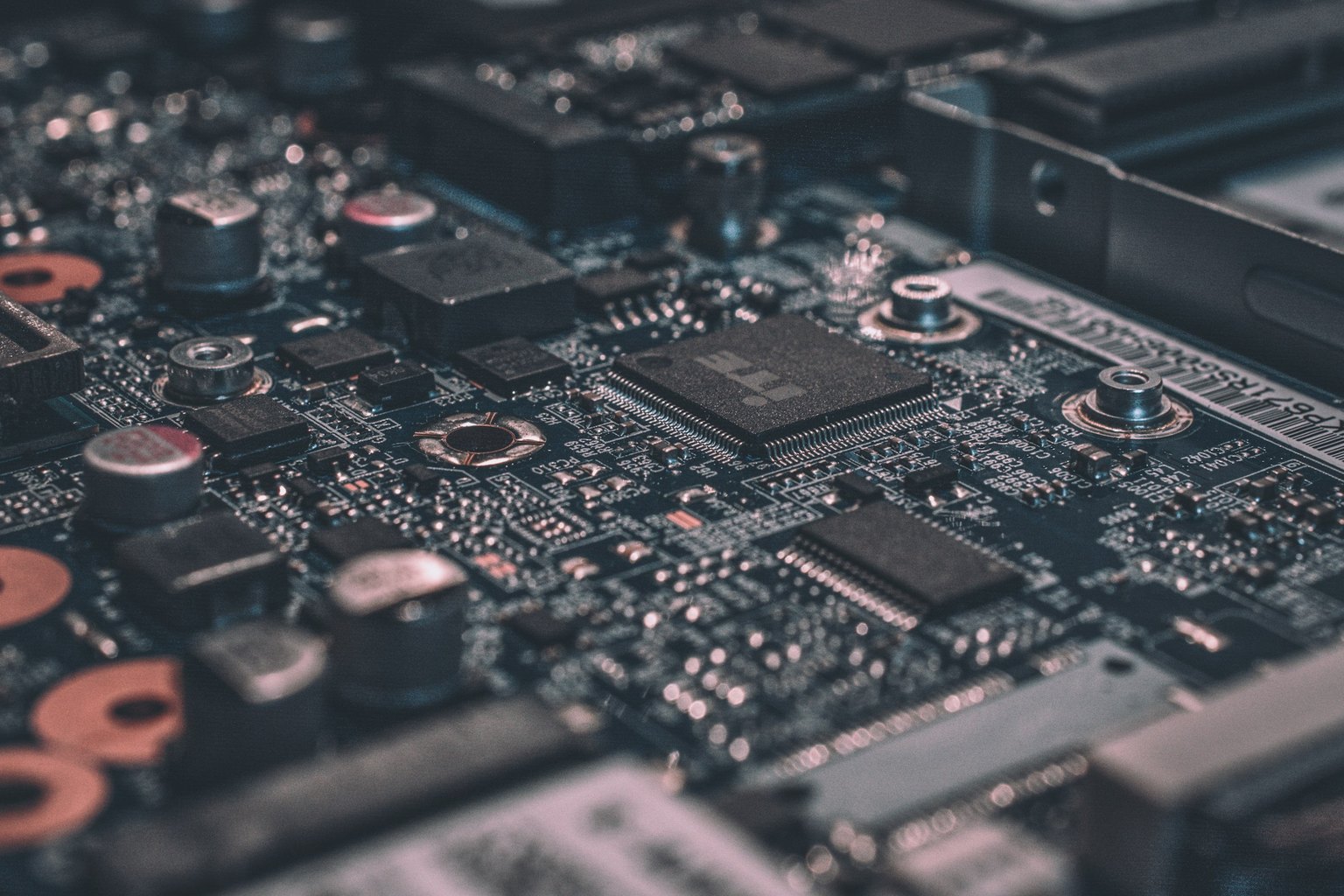
Building India's complete electronics ecosystem — through innovation, integration, and the T5 Concept that takes us from raw material in the ground to finished product in your hand.
India imports the majority of its electronic components and base materials. We exist to change that — by building, stage by stage, the integrated domestic value chain that turns raw materials into world-class finished electronics.
Headquartered in Delhi, PCB Design & Manufacturing Services combines deep technical engineering with commercial strategy and supply-chain architecture to strengthen Indian manufacturing for the long term.
Read our story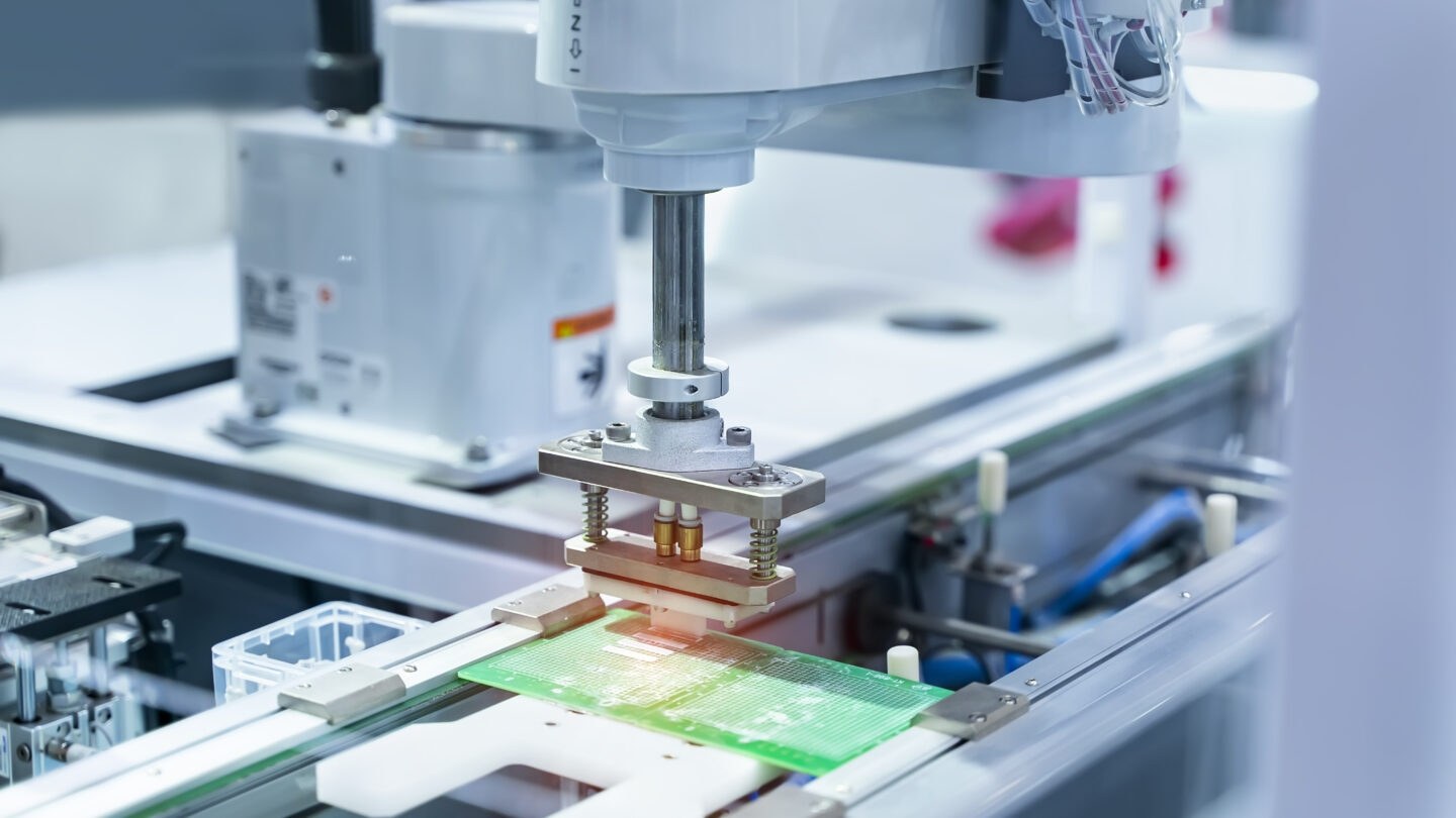
The T5 Concept is our core philosophy: build every link of the electronics value chain inside India — reducing import dependency and establishing the nation as a global manufacturing powerhouse.
Multilayer, HDI, high-speed, RF, automotive, industrial, telecom and defense-grade printed circuit boards engineered to international standards.
View solutionsCopper clad laminates, copper foil, glass fabric and resin systems — the foundational materials of every circuit board, developed for domestic supply.
Explore materialsTelecom, automotive, industrial automation, defense, aerospace, medical, consumer, renewable energy and the EV ecosystem.
See industriesBuilding a self-reliant electronics ecosystem takes more than manufacturing — it takes deep research across every layer of the value chain. We are developing capability and know-how in six strategic areas.
Advanced printed circuit board design and process research — multilayer, HDI, high-speed and high-reliability boards for demanding applications.
Research into IC packaging substrates — the high-density interconnect layer between silicon and the board that India must localise for true semiconductor independence.
Electrodeposited and rolled copper foil research — the conductive foundation of every laminate and the first metallurgical link in the chain.
Assembly, Test, Marking and Packaging research — the critical back-end of semiconductor production and a high-value entry point for Indian capability.
Sourcing and processing research for the base metals and minerals — copper, silica and specialty elements — that begin the electronics value chain.
Foundry and wafer-fabrication research — studying the processes and partnerships needed to bring front-end semiconductor manufacturing to India.
India is the world's fastest-growing major electronics market, backed by national policy momentum, a vast engineering talent base, and rising global demand for supply-chain diversification.

Parvez Ansari brings together technical depth, commercial strategy and supply-chain architecture to pursue a singular goal: a self-reliant Indian electronics industry built to last.
"Real industrial strength is not built overnight, and it is not built by importing finished goods. It is built link by link — materials, laminates, boards, components, assemblies — until the entire chain stands on Indian soil."
Parvez Ansari
Founder · Technical Visionary & Supply Chain Architect
Read the founder's vision